1 理论
对于半导体材料,其光学带隙和吸收系数之间的关系式为[1]: \alpha{h}\nu=B(h\nu-E_g)^m 其中\alpha为摩尔吸收系数,h为普朗克常数, \nu为入射光子频率,B为比例常数, E_g为半导体材料的光学带隙, m的值与半导体材料以及跃迁类型相关:
- 当 m=1/2 时,对应直接带隙半导体允许的偶极跃迁;
- 当 m=3/2 时,对应直接带隙半导体禁戒的偶极跃迁;
- 当 m=2 时,对应间接带隙半导体允许的跃迁;
- 当 m=3 时,对应间接带隙半导体禁戒的跃迁。
P.S. From http://www.cailiaoniu.com/78213.html
2 An example
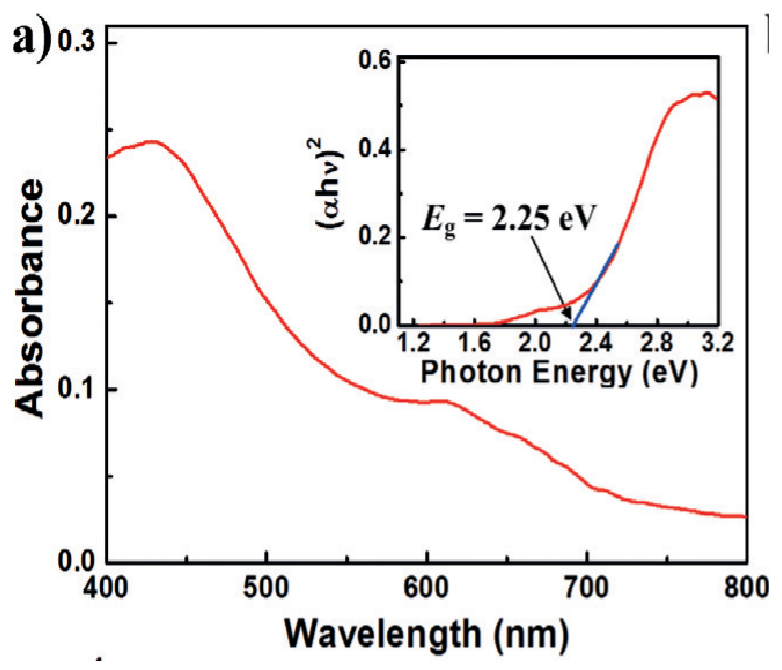
[2]The optical properties of the \gamma-B28 monolayer on a quartz substrate were analyzed by UV/Vis absorption spectroscopy (Figure 4a). A characteristic absorption peak, \lambda_{onset} , was observed at 614 nm (phonon energy 2.05 eV), which could be attributed to a direct excitonic transition. The corresponding optical band gap (Eg,op) was estimated to be 2.25 eV according to (\alpha h\nu)^2=h\nu-E_g, where h\nu is the corresponding phonon energy, and \alpha is the absorbance. This value is much higher than that of the corresponding bulk phase measured either by near-infrared optical absorption spectroscopy or calculated by first-principles calculations (1.7 eV), which is due to the presence of strong quantum-confinement effects in the monolayer.

- UV/Vis absorption spectrum of a monolayer \gamma-B28 film. Inset: (\alpha h\nu)^2 as a function of h\nu for band gap determination.
Ref.